
現在,您已準備好將 IP 核心整合至周邊的 FPGA 設計中。這 基本上意味著要在目標硬體的資料通訊協定 與 IP 核心介面上的協定之間,實作並連接轉換器。特別是,您需要 留意如何連接外部介面,例如記憶體控制器、感測器介面以及資料 輸出。
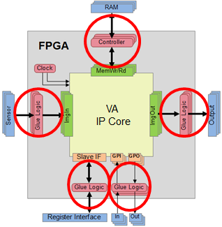
當您產生 IP 核心黑盒(如「為 IP 核心產生 VHDL 程式碼」一節所述)時,不僅是 IP 核心黑盒本身被 產生。在同一步驟中,系統還會產生一個完整的測試平台,該平台已針對測試 IP 核心的各個介面進行了客製化,以便您在將其整合至 HDL 設計時進行測試。
該測試平台可在 HDL 整合過程中,透過 IP 核心介面 模擬資料通訊。為 HDL 模擬所生成的工具,主要著重於測試介面 通訊協定,並為頂層 架構(您的 HDL 設計)中連接至該核心的電路產生刺激訊號。
在測試平台中,每個 個別介面埠 (日後可能 透過相應的VisualApplets 運算子進行連接)均 均會 獨立地,並由檔案 I/O 驅動。該模擬實體由以下 元件組成:
-
用於寄存器存取的從機介面模擬: 透過 檔案進行配置,此模擬模組提供一組可讀寫的寄存器。其中 設有專用寄存器,用於連接使能與重置訊號。 您可以設定 不同的處理程序。影像處理應用程式的實際處理程序數量將 於稍後(整合後)在VisualApplets 設計中定義。進行模擬時,請依照「從屬介面模擬」一節所述 來定義處理程序數量。使能與 重置是唯一連接至其他模擬模組的訊號,而這些模擬模組所屬的 處理程序,可透過模擬實體參數進行指定(詳見下文)。 寄存器 介面模擬器提供了一項功能,可根據 刺激檔隨時間變化調整寄存器值。在刺激檔中,您可以設定一個值,並定義該值應在何時 變更(例如:先設定為 1,經過 10,000 個時鐘週期後再設定為 0)。
-
連接至 ImgOut 埠的影像來源模擬器。此類 模組透過檔案驅動,將影像資料輸出至 IP 核心的 ImgOut 介面。您 可根據為影像輸出埠所指定的影像通訊協定,來設定此影像通訊協定 ID。
-
連接至 ImgIn 埠的幀匯出器模擬器。此類模組模擬一個 連接至 IP 核心 ImgIn 介面的運算子。您可以 根據為影像輸入埠所指定的影像協定,來設定此影像協定 ID。該 模組會將接收到的資料寫入檔案。
-
記憶體埠模擬器,其運作方式如同連接了一個使用 RAM 的模組。 寫入與讀取存取的順序由檔案模擬,而讀取到的資料則輸出至檔案。
-
GPIO 模擬器。每個用作輸出的 GPIO 訊號皆由一個訊號產生器驅動,該產生器 由一個檔案進行配置。每個 GPIO 輸入訊號均會被監控,而訊號的變化會 寫入報告檔案中。
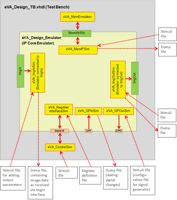
For RTL level simulation, a VHDL file eVA_Design.vhdl has been created. This file contains a package with name eVA_<PLATFORMNAME> ( <PlatformName> is the platform name you defined as described in 'Entering Platform Details'). This package contains two components:
-
eVA_Design:Visual Applets IP 核心的黑色盒子
-
eVA_Design_Emulator: Visual Applets IP 核心模擬器:此模擬器 為模擬測試平台實作基於檔案的刺激訊號產生功能。
以下顯示檔案 eVA_Design.vhdl 中的程式碼,此程式碼將 針對僅包含用於寄存器 存取之從屬介面的最簡單 VA IP 核心所 產生:
       component eVA_Design
       generic(

              RegIFDataWidth : integer := 32;
              RegIFAddrWidth : integer := 16);

       port(

              iDesignClk: in std_logic := '0';
              iDesignClk2x: in std_logic := '0';

              ivRegWrData: in std_logic_vector(RegIFDataWidth-1 downto 0) := (others=>'0');
              ivRegWrAddr: in std_logic_vector(RegIFAddrWidth-1 downto 0) := (others=>'0');
              iRegWrValid: in std_logic := '0';

              ivRegRdAddr: in std_logic_vector(RegIFAddrWidth-1 downto 0) := (others=>'0');
              iRegRdValid: in std_logic := '0';
              ovRegRdData: out std_logic_vector(RegIFDataWidth-1 downto 0) := (others=>'0');
              oRegRdDataValid: out std_logic := '0'

       );
       end component;

       component eVA_Design_Emulator
       generic(

              RegIFDataWidth : integer := 32;
              RegIFAddrWidth : integer := 16;
              NrOfProcesses: integer := 2;
              RegisterDefinitionFile: string := ""

       );
       port(

              iDesignClk: in std_logic := '0';
              iDesignClk2x: in std_logic := '0';

              ivRegWrData: in std_logic_vector(RegIFDataWidth-1 downto 0) := (others=>'0');
              ivRegWrAddr: in std_logic_vector(RegIFAddrWidth-1 downto 0) := (others=>'0');
              iRegWrValid: in std_logic := '0';

              ivRegRdAddr: in std_logic_vector(RegIFAddrWidth-1 downto 0) := (others=>'0');
              iRegRdValid: in std_logic := '0';
              ovRegRdData: out std_logic_vector(RegIFDataWidth-1 downto 0) := (others=>'0');
              oRegRdDataValid: out std_logic := '0'

       );
       end component;
有關模擬各類 IP 核心介面的更詳細資訊, 請參閱以下各小節。
eVA 設計模擬器有一個參數 NrOfProcesses。此 參數為 1 至 16 之間的整數。該參數的作用是建立一組 用於重置及啟用設計的預定義寄存器。以下地址 將會被設定:
-
0x00:全系統重置
-
0x01:全域啟用
-
0x02 * (i+1): Process Reset for process i (i < NrOfProcesses).
-
0x02 * (i+1) + 0x01: Process Enable for process i (i < NrOfProcesses).
因此,當 NrOfProcesses = 2 時,從屬介面位址空間的前 6 個位址 將用於控制模擬設計的重置與啟用。每個影像埠將 對應一組由上述寄存器控制的重置與啟用訊號。 整合完成後,VisualApplets 的使用者將把介面與某個程序關聯起來,方法是 將運算子實例化為程序的元件,並將此運算子實例連接至 介面。
用於寄存器存取的從屬介面模擬器,會透過一個 文字檔案進一步進行配置,該檔案由實體參數 RegisterDefinitionFile 設定,其設定方式如 上述 VHDL 程式碼所示。此參數會在「黑盒」及測試平台 生成過程中自動設定,詳情請參閱「為 IP 核心生成 VHDL 程式碼」一節。
寄存器定義檔中可能會包含以下指令:
|
命令 |
描述 |
|---|---|
|
REM |
行中剩餘的部分為註解 |
|
DEF |
定義寄存器。此指令的語法如下: DEF <addr> <width> <write_read> <init_value>
參數如下: <init_value>: hexadecimal initial value <addr>: hexadecimal value of register address <width>: bit width of register <write_read>: 1 for write register, 0 for read register |
|
CON |
將寫入寄存器與讀取寄存器連接。此指令的 語法如下: CON <wrRegAddr> <rdRegAddr>
參數如下: <wrRegAddr>: address of write register (hex) <rdRegAddr>: address of read register (hex) |
|
WCK |
等待若干個時鐘週期。語法如下: WCK <clock_ticks>
with <clock_ticks> giving the number of clock ticks in hexadecimal format. |
|
SET |
設定讀取寄存器的值 SET <rdRegAddr> <value>
參數如下: <rdRegAddr>: address of read register (hex) <value>: hexadecimal register value |
在任何指令的最後一個參數之後,您可以加上以「#」開頭的註解。
以下程式碼是一個登錄檔定義範例,用於配置兩個寫入 和兩個讀取登錄檔,其中一個讀取登錄檔(位址 0x7)會在 16 個時脈週期後預設值,而另一個讀取登錄檔(位址 0x6)則由位址 0x6 的寫入登錄檔驅動:
      REM ************************************************************
      REM Command formats: DEF <addr> <width> <write_read> <init_value>
      REM                  CON <wrRegAddr> <rdRegAddr>
      REM                  WCK <clock_ticks>
      REM                  SET <rdRegAddr> <value>
      REM ************************************************************
      DEF 0006 10 1 00000000 #define write reg with width 0x10 at address 0x6
      CON 0006 0006          #create read reg with addr 0x6 connected to
      REM                     write register with address 0x6
      DEF 0007 20 1 00000000 #define write reg with width 0x20 at address 0x7
      DEF 0007 10 0 00000000 #define read register at address 0x7
      WCK 0010               #wait for 16 clock cycles
      SET 0007 0000000C      #set read register value
ImgOut 類型的影像通訊介面模擬,是由一個刺激 檔案驅動的,該檔案提供有關資料輸出序列的資訊。
For any present ImgOut port, the eVA_Design_Emulator entity has a generic <PORTIDX>_StimuliFileName where <PORTIDX> is the name of the corresponding image output port class followed by the port number. Each line within the given file must follow the syntax
<Command> <Data> <EndOfLine> <EndOfFrame> <DataValid>
where <Command> is a three letter command, <Data> provides an hexadecimal data word, and the three remaining parameters correspond to the image protocol flags.
下表說明可用的指令:
|
命令 |
描述 |
|---|---|
|
DAT |
資料指令。此指令提供將作為該埠輸出資料的資料
|
|
WCK |
等待指令。參數 |
|
FID |
設定 FID 輸出。此參數 |
|
PDX |
將第 X 個埠的參數輸出設定為隨附的值
|
在任何命令列前,都可以加上以「#」開頭的註解。
以下程式碼是一個範例刺激檔,會先輸出一張 3x2 的圖像, 接著進行參數變更(包含 FID),並輸出第二張尺寸為 3x1 的圖像:
      DAT 00000000 0 0 0 #Format: Cmd Data(hex) EndOfLine EndOfFrame DataValid
      DAT 0000001a 0 0 1
      DAT 0000001b 0 0 1
      DAT 0000001c 0 0 1
      DAT 00000000 1 0 1
      DAT 0000002a 0 0 1
      DAT 0000002b 0 0 1
      DAT 0000002c 0 0 1
      DAT 00000000 1 1 1
      WCK 00000004 0 0 0
      FID 00000001 0 0 0
      PD0 00000011 0 0 0
      PD1 00000022 0 0 0
      PD2 00000033 0 0 0
      WCK 00000001 0 0 0
      DAT 0000003a 0 0 1
      DAT 0000003b 0 0 1
      DAT 0000003c 1 1 1
      DAT 00000000 0 0 0
      DAT 00000000 0 0 0
      DAT 00000000 0 0 0
The reset and enable ports of the concerning image communication interface are connected to dedicated registers of the slave interface where the affiliation to a process is done according to a parameter <PORTIDX>_ProcessID.
ImgIn 類型的影像通訊介面的模擬,是由一個刺激 檔案驅動的,該檔案提供了有關參數狀態序列的資訊。
For any present ImgIn port, the eVA_Design_Emulator entity has a generic <PORTIDX>_StimuliFileName where <PORTIDX> is the name of the corresponding image input port class followed by the port number. The syntax is exactly the same as in the case of the stimuli for ImgOut interfaces except that no DAT command is available. A simple stimuli file may look like,
      WCK 00000010 0 0 0    #Format: Command Data(hex) EndOfLine EndOfFrame DataValid
      FID 00000001 0 0 0
      PD0 00000111 0 0 0
      PD1 00000222 0 0 0
      PD2 00000333 0 0 0
      WCK 00000001 0 0 0
where the parameters <EndOfLine>,<EndOfFrame> and <DataValid> are actually meaningless.
The ImgIn interface emulator writes the received data to file. For that purpose the eVA_Design_Emulator entity has a generic <PORTIDX>_DumpFileName. During simulation, a file with the given name is created and the data is written using DAT and WCK commands in a format which exactly corresponds to the stimuli file format for an ImgOut interface emulator.
The reset and enable ports of the concerning image communication interface are connected to dedicated registers of the slave interface where the affiliation to a process is done according to a parameter <PORTIDX>_ProcessID.
記憶體通訊的模擬是由一個刺激檔案驅動的,該檔案 提供了有關存取順序的資訊。
For any present memory port, the eVA_Design_Emulator entity has a generic Mem<X>_StimuliFileName where <X> is the port number. The stimuli file consists of lines with following syntax,
<WrData> <WrAddr> <WrFlag> <WrReq> <RdAddr> <RdFlag> <RdReq>
其中各項的含義如下:
<WrData>: hexadecimal data word intended for port ovMemWrDataX
<WrAddr>: hexadecimal write address (for ovMemWrAddrX)
<WrFlag>: hexadecimal write flag (for ovMemWrFlagX)
<WrReq>: write request (oMemWrReqX)
<RdAddr>: hexadecimal read address (for ovMemRdAddrX)
<RdFlag>: hexadecimal read flag (for ovMemRdFlagX)
<RdReq>: read request (oMemRdReqX)
在任何命令列中,您都可以添加以「#」開頭的註解。
以下程式碼是一個範例刺激檔,會產生兩張圖片, 每張圖片均由四個資料字組成:
      0000000000000000 000000 0 0 000000 00 0
      0000000000000000 000000 0 0 000000 00 0
      0000000000000000 000000 0 0 000000 00 0
      0000000000000000 000000 0 0 000000 00 0
      000000000000000a 000000 0 1 000000 00 0 #Write 0xa to address 0x0
      000000000000000b 000001 0 1 000000 00 0 #Write 0xb to address 0x1
      000000000000000c 000002 0 1 000000 00 0 #Write 0xc to address 0x2
      000000000000000d 000003 1 1 000000 00 0 #Write 0xd to address 0x3
      0000000000000000 000000 0 0 000000 00 0
      0000000000000000 000000 0 0 000000 00 0
      0000000000000000 000000 0 0 000000 00 0
      0000000000000000 000000 0 0 000000 00 0
      0000000000000000 000000 0 0 000000 00 0
      0000000000000000 000000 0 0 000000 00 0
      000000000000000e 000104 1 1 000000 00 0 #Write 0xe to address 0x10a
      00000000000000bb 000001 0 1 000000 00 0 #Write 0xbb to address 0x1
      0000000000000000 000000 0 0 000000 00 1 #Read from address 0x0
      0000000000000000 000000 0 0 000001 00 1 #Read from address 0x1
      0000000000000000 000000 0 0 000002 00 1 #Read from address 0x2
      0000000000000000 000000 0 0 000003 01 1 #Read from address 0x3
      000000000000000e 000000 0 0 000104 00 1 #Read from address 0x104
      0000000000000000 000000 0 0 000000 00 0
      0000000000000000 000000 0 0 000000 00 0
      0000000000000000 000000 0 0 000000 00 0
Read data returned from the memory to the emulator is written to a file. For providing the file name the eVA_Design_Emulator entity has a generic Mem<X>_DumpFileName. The dump lines have the following format,
<RdData> <RdFlag>
其中各項的含義如下:
<RdData>: hexadecimal data word according to port ivMemRdDataX
<RdFlag>: hexadecimal value of read flag according to port ivMemRdFlagX
專用輸出信號的模擬是針對每個信號分別進行,並由 一個刺激檔案驅動。該檔案中提供了關於信號狀態序列的資訊。
The stimuli file may consist of a number of commands which are described below. For any present output signal port the eVA_Design_Emulator entity has a generic oSig_<NAME>_StimuliFileName where <NAME> is the concerning port name.
下表說明可用的指令:
|
命令 |
描述 |
|---|---|
|
SET |
設定訊號。此指令指定輸出端 oSig_NAME 的輸出將被設定為該訊號狀態。下一條指令將在 一個時脈週期後執行。其語法為 SET <value>
where <value> may be 0 or 1. |
|
WCK |
「等待」指令。其語法如下: WCK <ticks
where the parameter <ticks> provides the number of clock ticks for which the signal will be held constant. |
|
RST |
從頭重新開始。指令解譯器將從刺激檔案的第一行重新開始。此指令沒有任何參數。該指令將在同一個時脈週期執行檔案的第一個指令,允許組合無間隙的迴圈。 |
|
STP |
在目前狀態停止。指令解譯器將停止,且目前的訊號狀態將保持常數,直到模擬結束。此指令沒有任何參數。 |
在任何命令列前,您都可以加上註解,註解前需加上「#’作為前綴。
以下程式碼是一個範例刺激檔,會使輸出訊號進行翻轉, 先維持低電平 5 個時鐘週期,再維持高電平 7 個時鐘週期(與 iDesignClk 同步):
      SET 0              # deassert output
      WCK 0004           # wait for 4 clock cycles
      SET 1              # assert output
      WCK 0006           # wait for 6 clock cycles
      RST                # restart from begin
Dedicated input signals are monitored writing a dump file iSig_<NAME>_DumpFileName where <NAME> is the concerning port name. The file is composed of SET and WCK commands exactly corresponding to the commands of the stimuli file for a dedicated output signal.
要嵌入 IP 核心:
-
將 IP 核心黑盒的所有介面整合至您的頂層 HDL 設計中。若要 在逐步實作的過程中測試這些介面,請使用 與黑盒一併產生的測試平台(如「模擬框架」一節所述)。
-
在將所有黑盒介面完全整合至您的 HDL 設計之後, 請產生該設計的網表。
-
建立一個約束條件檔案。
在實際產生 eVA 外掛程式(該外掛程式將把您的硬體專用 IP
核心及其所有介面規格導入VisualApplets )之前,您需要先在硬體描述檔中
補充一些詳細資訊(*.xml 或
*.eva) 透過 的 圖形使用者介面 eVA Designer:
-
啟動VisualApplets 並開啟 。
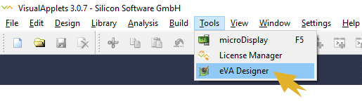
-
前往 分頁。
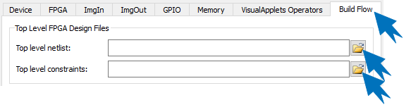
-
位於 下,輸入您所建立的檔案路徑:
請指定頂層網表的路徑 (此為您整體 FPGA 設計的網表,其中包含已封裝的VisualApplets 核心黑盒)。
請指定頂層網表(包含封裝好的 VisualApplets 核心黑盒子在內的整體 FPGA 設計網表)的用戶約束檔案路徑。若您使用Xilinx ISE 工具鏈,此路徑為
*.ucf檔案, 如果您使用的是Xilinx 的 Vivado 工具鏈,這是一個*.xdc檔案。 -
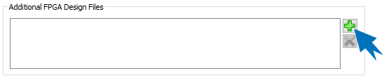
在 下,如有需要,請指定這些檔案的路徑。此類 檔案可能是其他 IP 核心的網表,以及相關的約束檔案等。
在 下,您現在需要指定將要使用的 工具鏈。位流合成需要第三方軟體:視 所使用的 FPGA 而定,可選的工具包括Xilinx Vivado WebPACK(免費)、 Xilinx Vivado Design Suite , Xilinx ISE WebPACK(免費),或Xilinx ISE Design Suite (Xilinx Corp. 的註冊商標)。
-
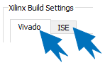
請選取 或 標籤,具體取決於您用於 合成 FPGA 位元流的Xilinx 工具鏈。
-
請輸入您的工具鏈詳細資訊。
:
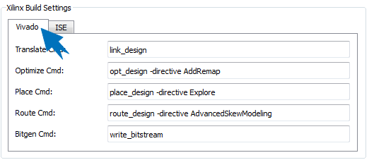
若您使用的是 VivadoXilinx ,請提供以下詳細資訊:
Vivado 實作流程中 link_design 步驟的命令列。
Vivado 實作流程中「opt_design」步驟的 命令列。
Vivado 實作流程中「place_design」步驟的 命令列。
Vivado 實作流程中 route_design 步驟的命令列。
Vivado 實作流程中「write_bitstream」步驟的命令列。
:
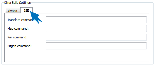
若您使用的是Xilinx ISE,請提供以下詳細資訊:
ISE 實作流程中「翻譯」步驟的命令列 。
ISE 實作流程中「映射」步驟的命令列 。
ISE 實作流程中「放置與路由」步驟的命令列 。
ISE 實作流程中,用於配置位元流 產生步驟的命令列。
-
在 下,請視需要輸入您希望 在VisualApplets 的硬體專用目錄中提供之附加檔案。此類檔案 可能包含使用者文件、建置流程外掛程式、腳本、文件、協助工具等。
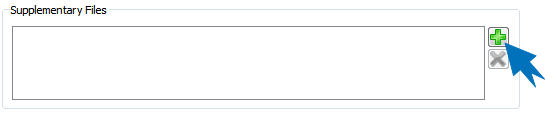
在您輸入完畢所有與建置流程相關的詳細資訊後,即可開始產生 適用於目標硬體的 eVA 外掛程式安裝程式。
適用於VisualApplets 的硬體專用 eVA 外掛程式是由以下 檔案所組成:
-
必填:
-
硬體描述檔 (
*.xml),包括運算子 定義(參見 「定義硬體特定運算子」) -
頂層網表,包含封裝好的 IP 核心黑盒 (
*.ngc/*.edn) (參見下方的方框) -
約束條件檔案 (
*.ucf格式(如果您使用 Xilinx ISE),*.xdc若您使用Xilinx Vivado),請採用此格式(參見下方的方框)
-
-
可選:
-
硬體裝置的圖示檔案(
*.png) 用於在VisualApplets 圖形使用者介面中 呈現硬體的圖形化表示 -
各硬體專用運算子的圖示檔案 (
*.png) 用於在 VisualApplets 圖形使用者介面中以圖形方式呈現運算子 -
特定平台運算子的說明檔案(
*.html)
-
您已將所有這些檔案輸入至 eVA Designer 在 執行「定義 IP 核心屬性」及 「輸入建置流程詳細資訊」兩節所述步驟的過程中。
![[注意]](../common/images/admon/note.png) |
VisualApplets IP 核心網表生成 |
|---|---|
|
您也可以在不使用頂層網表和約束檔案的情況下建立外掛程式安裝程式。 安裝完成後,您將能在VisualApplets 看到整合後的樣貌 (包含可用的硬體專用運算子等)。 然而,若外掛程式中未包含頂層網表及約束條件檔案, 您將無法建構能在您的硬體平台上執行的應用程式。 |
要為VisualApplets 建置實際的 eVA 外掛程式,您有兩種選擇。您可以
-
編譯並立即將 eVA 外掛程式安裝至 您電腦上的VisualApplets 安裝環境中。
-
建立一個可執行檔形式的 eVA 外掛程式安裝程式,以便提供給同事和/或 客戶。
如果您想在開發該外掛程式的電腦上直接測試或使用它, 請:
-
在 中,開啟 選單。
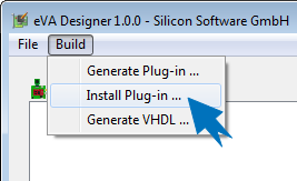
-
選取選單項目
-
請輸入您的VisualApplets 安裝目錄路徑,或確認 建議的安裝目錄。

系統已通知您安裝成功:

您可以在VisualApplets 安裝目錄中的 子目錄內找到該外掛程式的檔案
eVA/platforms/<devicename>:
若要建立一個可執行檔,以便將其轉交給VisualApplets 的開發人員,由他們 為您的硬體設計影像處理應用程式:
-
在 中,開啟 選單。
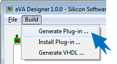
-
選取選單項目
-
請選擇您要儲存外掛的目標資料夾。
一旦您選取目標資料夾,eVA 外掛程式便會立即建立。系統會 透過訊息通知您,表示建置已成功:
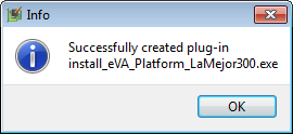
該外掛程式位於指定資料夾中:
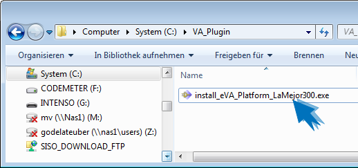
現在您可以發行此外掛程式了。
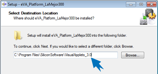
安裝完成後,您可以在 VisualApplets 上,為您的平台設計新的影像處理應用程式:
-
開啟VisualApplets 。
-
從「檔案」選單中,選擇 。
現在,您可以選擇硬體平台,並在VisualApplets 開始進行設計:
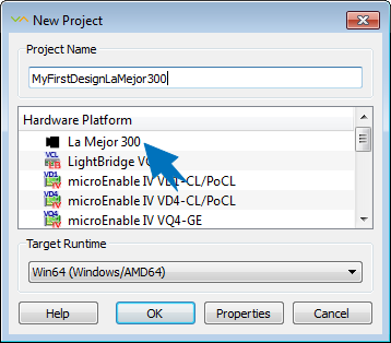
如需瞭解如何使用 VisualApplets 設計影像擷取與處理應用程式,請參閱詳盡的VisualApplets 線上文件,網址為 《入門指南》。
 上一頁
上一頁

